Electronics Design
Schematics:
This week assignement is to redraw an "echo hello-world board" & add a LED & a button to it.
To do this i use the same workflow i use on Week 4.
I chose to work on the ATtiny 44 hello-board with the objectif: "making it smaller."
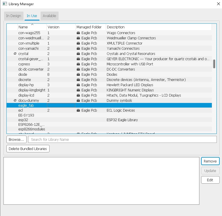


I start by dowload the Fablibrary to have a nice and easy library to work with, & install it with the library manager on Eagle.
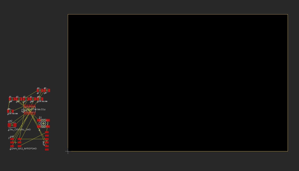
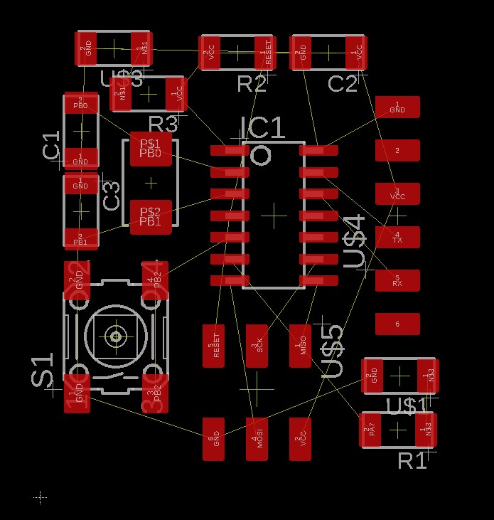
After that i do my schematic, i add to the original board a "on tensions"LED, a button on PB2 & a LED on PA7. (I add a curren-limiting resistor for each LED.)
When i finished my Schematic i do a Electrical Rules Check, it's Ok let's go prepare the Board.
Board:
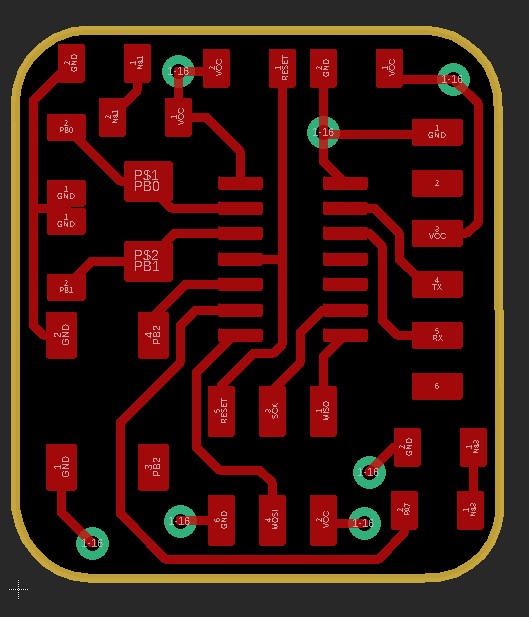
When i switch betwen schematics to board, eagle give me a nice Blackboard and all my nessecary composant in a stack on the side.
here we go, let's try to do something clear & compact.
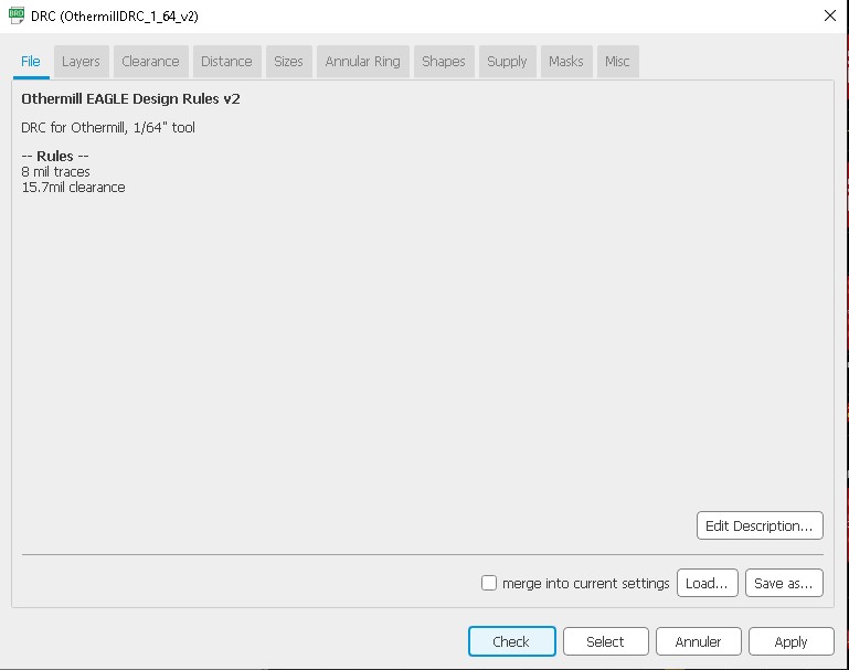
On Week 4 i already charge on Eagle the Design Rules Check list used by the Othermill CNC. Before placing my composant i check the good rules are activate.
For this project i choose to work with a 1/64" flat end mill as my smallest mill i chose for this reason the 1/64" DRC for the othermill machine.
Now Try to place the composant with some logic for a better routting work.
For a Easy work on this compacting way i chose to work in a "Two-side" PCB for this i add some VIA ( is an electrical connection between layers in a physical electronic circuit "wikpedia")
For this i'm going to use some special rivets, due to the dimension of the rivets (0.6mm diameter) i setup my VIA for a 0.7mm hole.


Now i could trace a VCC & a GND route on the bottom face, connecting the VIA for my different need on the top face.
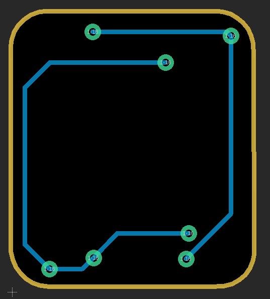
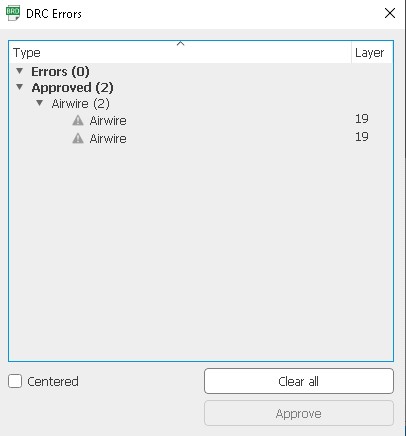
Before finishing i Run a check of the DRC to see if i made some mistake. (I approved two airwire, cause EAGLE want i connect the two side of the button but the button do this by it self.)

The files here for the Schematic & the Board
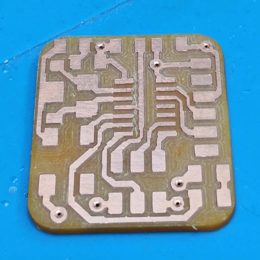
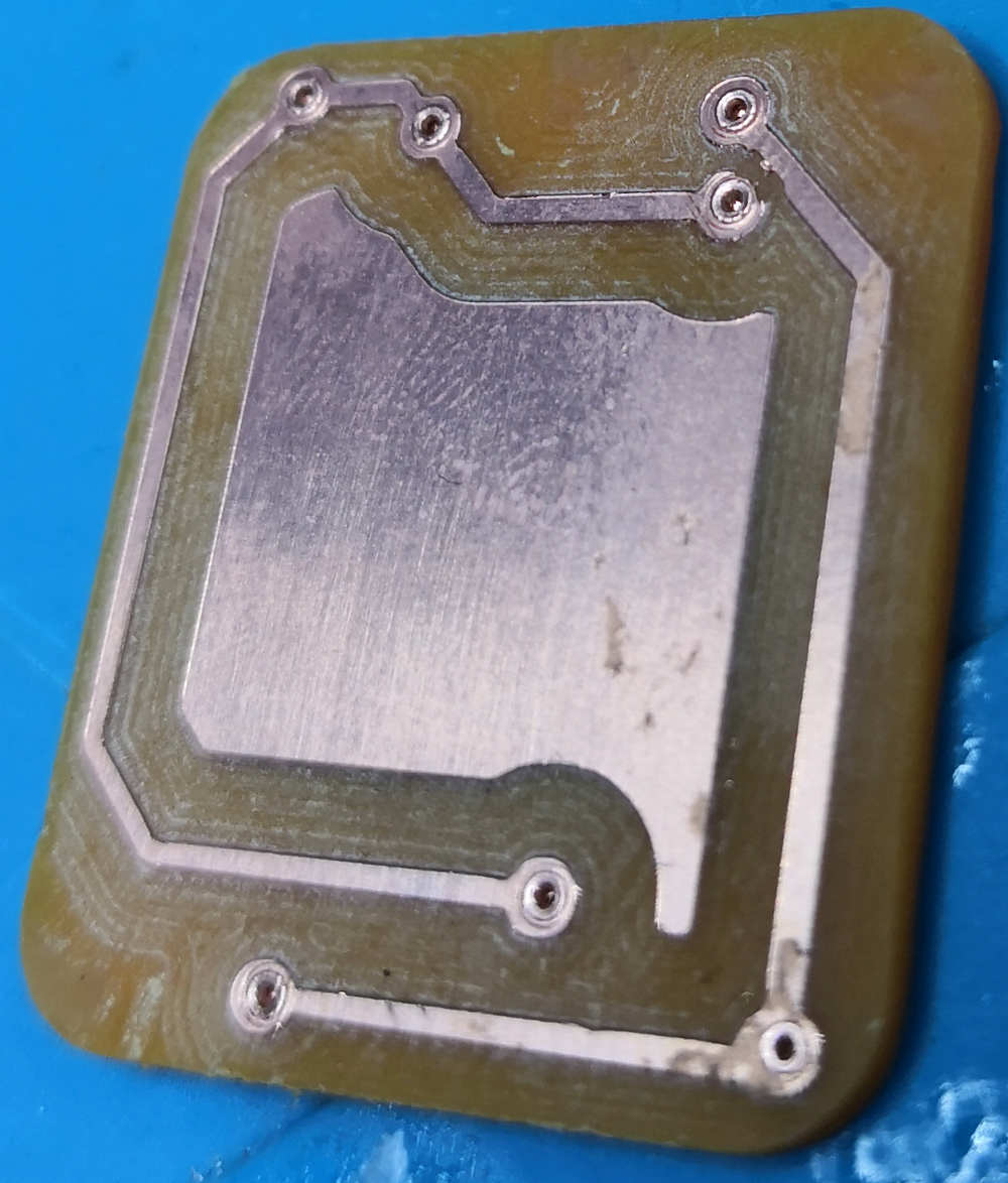
Milling on a double sided pcb it's quite tricky: (sorry, i forgot to take pictures of this work)
- starting by milling the bottom trace of the board (like on Week 4) by placing the pcb on the bottom right corner of the Machine
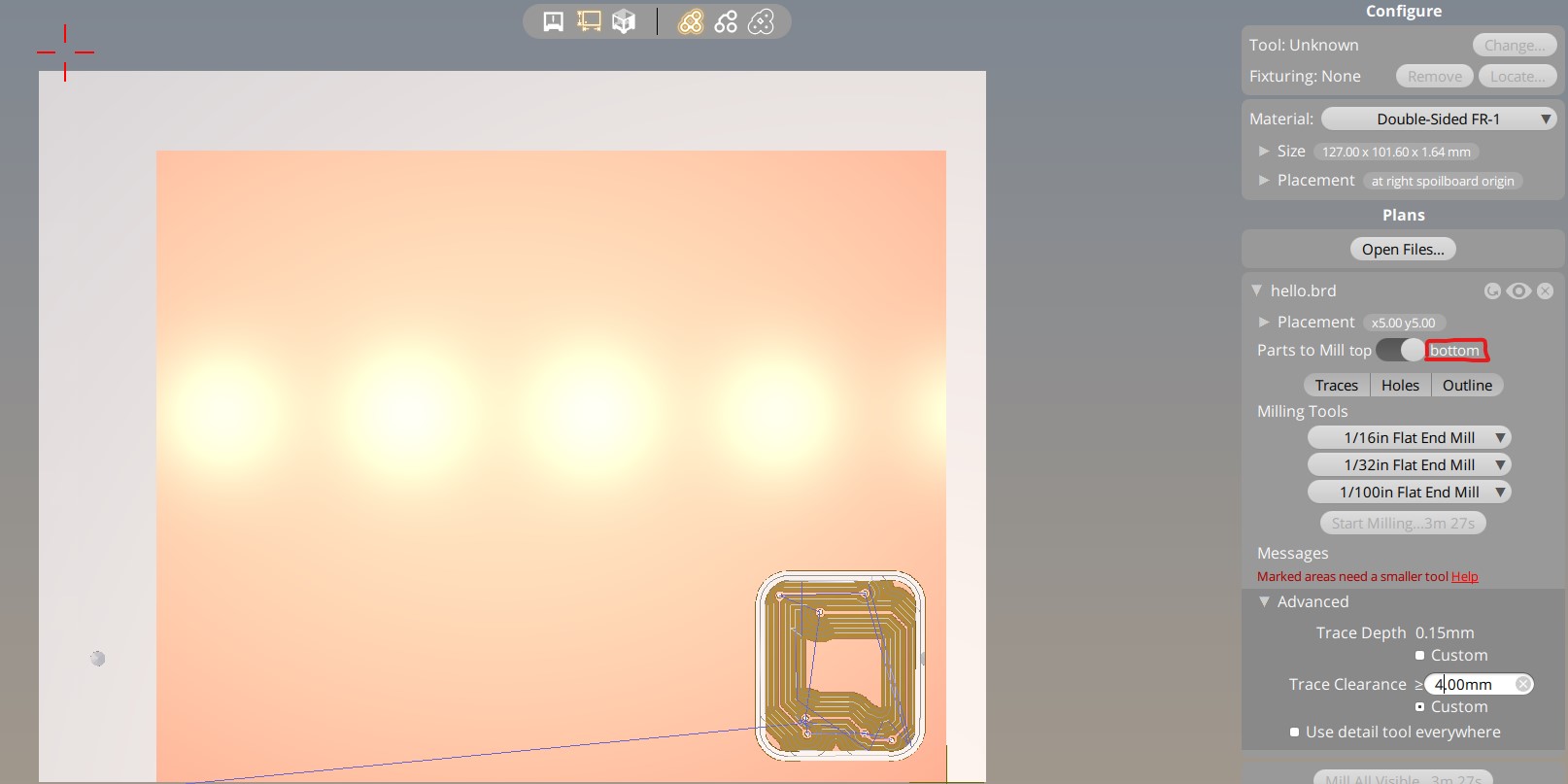
- After that take of the tape on the first side, Upside Down your board and replace the board on the bottom left corner of the machine (take really care to have a good placement, if not you have a gap between up & bottom when drilling the VIA holes)
After milling the PCB, i use some copper rivet to allow the current to pass by the VIA, using the special tool.
It's really pleasant to use this rivets but quite tricky on start due to the really tiny size. It's doing a very nice finished loock to the PCB.


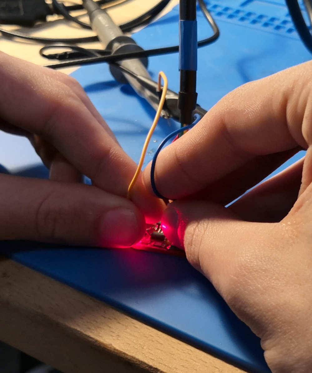
After that, i solder all my composant on the board.
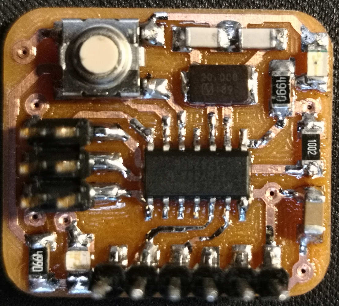
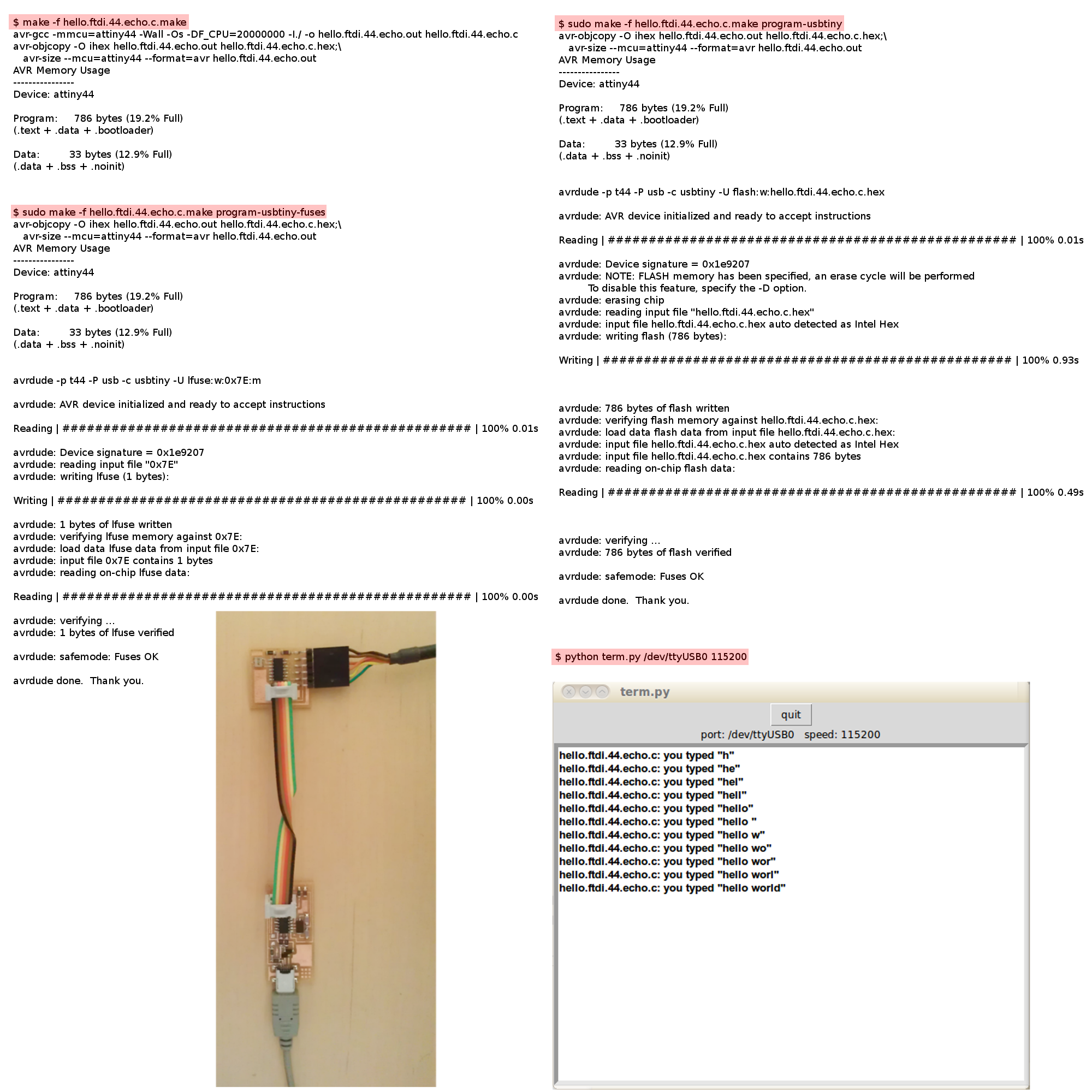
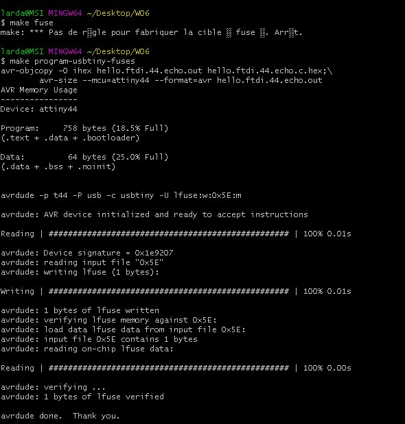
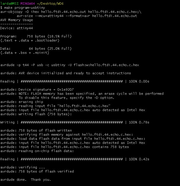
Testing & Programming the Board
I use a Multimeter to check the continuity off all my traces and to mesure the resistances & the capacitor value. All seem OK, great.
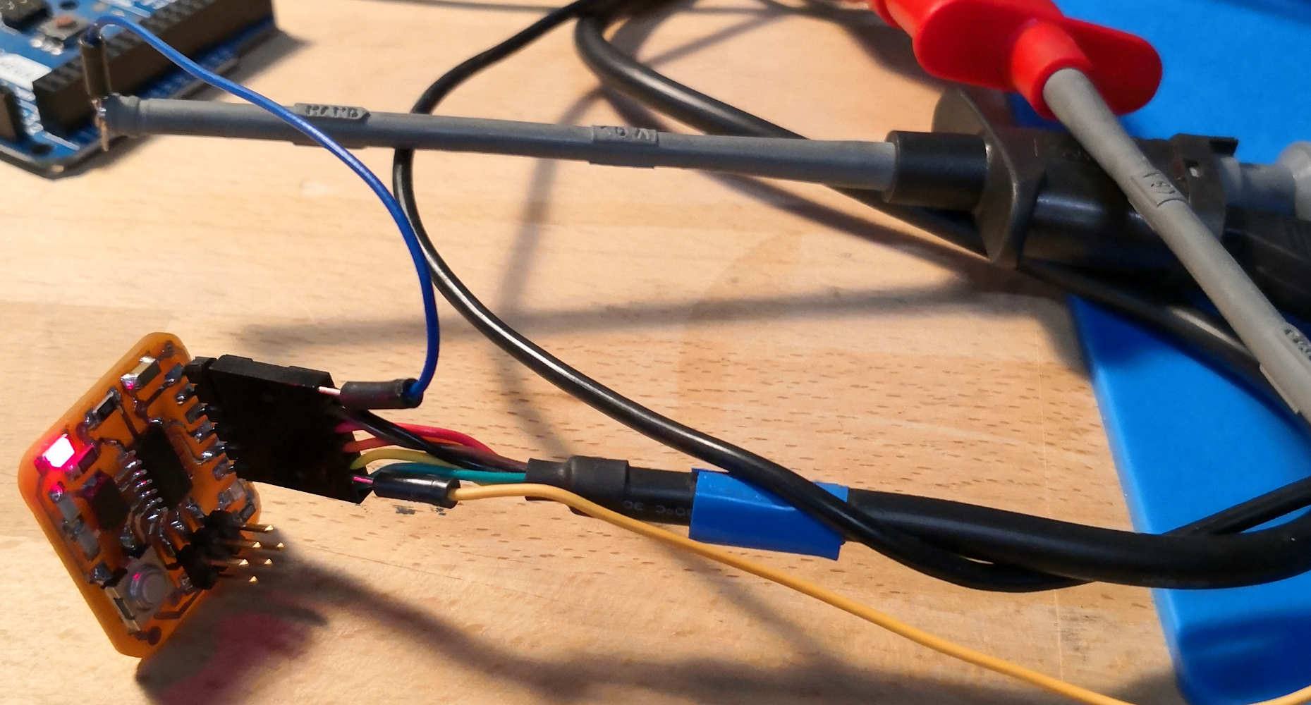
I use my USBtinyISP made on Week 4 for programming & a FTPI cable to supplying power and Serial communications.
I try a lot of different solutions without result & give a great Thanks to Jonah at "DIGISCOPE", he give to me the solutions.
After dowload the "echo.c" file & the "echo.c.make"
one
i have to rename the last one on "makefile" & let's go just following this TUTO.

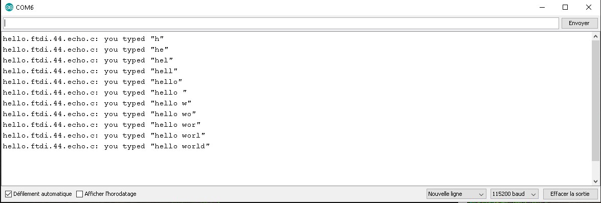
A short video of the Echo working:
Group Asssignement:
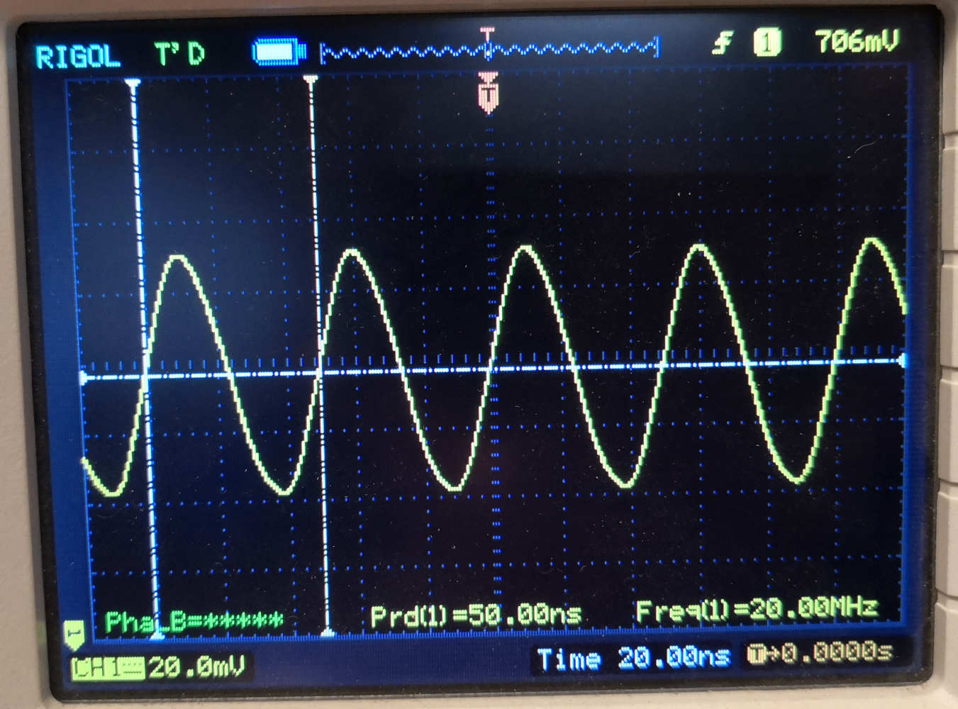
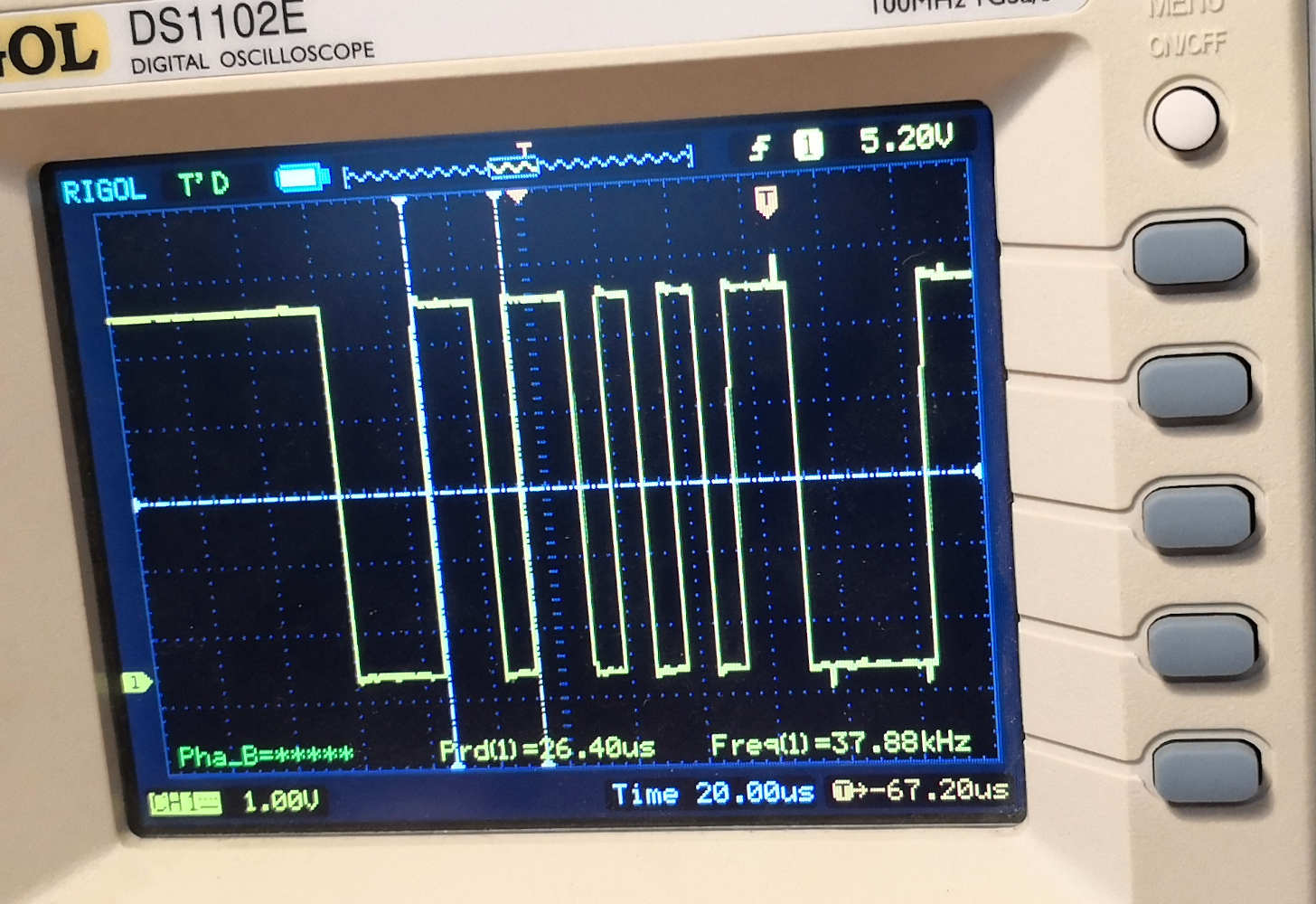
With Alban we using the Oscilloscope to observe some operation of my board.
- First we looking the external clock signal.(not so easy on this small board to prob the signal ^^)
- In a second time we looking the "l" letter send in the Echo programme.
- And for the fun we testing the "Fading" sketch on a LED with an arduino to see the PWM change.
Bonus
Take a look to my Final Project PCB design here.